- 您现在的位置:买卖IC网 > Sheet目录333 > IRS21864STRPBF (International Rectifier)IC DRIVER HI/LO SIDE 600V 14SOIC
�� �
�
�IRS2186(4)(S)PBF�
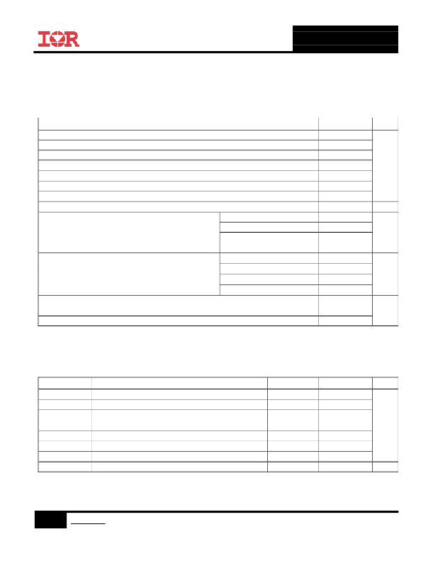
�Absolute� Maximum� Ratings�
�Absolute� maximum� ratings� indicate� sustained� limits� beyond� which� damage� to� the� device� may� occur.� All� voltage�
�parameters� are� absolute� voltages� referenced� to� COM.� The� thermal� resistance� and� power� dissipation� ratings� are�
�measured� under� board� mounted� and� still� air� conditions.�
�Symbol�
�V� B�
�V� S�
�V� HO�
�V� CC�
�V� LO�
�V� IN�
�V� SS�
�dV� S� /� dt�
�Definition�
�High� side� floating� absolute� voltage�
�High� side� floating� supply� offset� voltage�
�High� side� floating� output� voltage�
�Low� side� and� logic� fixed� supply� voltage�
�Low� side� output� voltage�
�Logic� input� voltage� (HIN� &� LIN)�
�Logic� ground� (IRS21864)�
�Allowable offset supply voltage transien� t�
�8� lead� PDIP�
�Min.�
�-0.3�
�V� B� -� 20�
�V� S� -� 0.3�
�-0.3�
�-0.3�
�V� SS� -� 0.3�
�V� CC� -� 20�
�—�
�—�
�Max.�
�?�
�620�
�V� B� +� 0.3�
�V� B� +� 0.3�
�?�
�20�
�V� CC� +� 0.3�
�V� CC� +� 0.3�
�V� CC� +� 0.3�
�50�
�1�
�Units�
�V�
�V/ns�
�P� D�
�Package� power� dissipation�
�@� T� A� ≤� +25°C�
�8� lead� SOIC�
�14� lead� PDIP�
�—�
�—�
�0.625�
�1.6�
�W�
�14� lead� SOIC�
�8� lead� PDIP�
�—�
�—�
�1�
�125�
�Rth� JA�
�Thermal� resistance,� junction� to�
�ambient�
�8� lead� SOIC�
�14� lead� PDIP�
�—�
�—�
�200�
�75�
�°C/W�
�14� lead� SOIC�
�—�
�120�
�T� J�
�Junction� temperature�
�—�
�150�
�T� S�
�T� L�
�Storage� temperature�
�Lead� temperature� (soldering,� 10� seconds)�
�-50�
�—�
�150�
�300�
�°C�
�Recommended� Operating� Conditions�
�The� input/output� logic� timing� diagram� is� shown� in� figure� 1.� For� proper� operation� the� device� should� be� used� within�
�the� recommended� conditions.� The� V� S� and� V� SS� offset� rating� is� tested� with� all� supplies� biased� at� 15� V� differential.�
�Symbol�
�V� B�
�V� S�
�V� HO�
�V� CC�
�V� LO�
�V� IN�
�V� SS�
�T� A�
�Definition�
�High� side� floating� absolute� voltage�
�High� side� floating� supply� offset� voltage�
�High� side� floating� output� voltage�
�Low� side� and� logic� fixed� supply� voltage�
�Low� side� output� voltage�
�Logic� input� voltage� (HIN� &� LIN)�
�Logic� ground� (IRS21864)�
�Ambient� temperature�
�Min.�
�V� S� +� 10�
�??�
�V� S�
�10�
�0�
�V� SS�
�-5�
�-40�
�Max.�
�V� S� +� 20�
�600�
�V� B�
�20�
�V� CC�
�V� CC�
�5�
�125�
�Units�
�V�
�°C�
�?�
�??�
�All� supplies� are� fully� tested� at� 25� V� and� an� internal� 20� V� clamp� exists� for� each� supply�
�Logic� operational� for� V� S� of� -5� V� to� 600� V.� Logic� state� held� for� V� S� of� -5� V� to� –� V� BS� (Please� refer� to� the� Design� Tip� DT97-3�
�for� more� details)�
�4�
�www.irf.com�
�?� 2013� International� Rectifier�
�April� 29,� 2013�
�发布紧急采购,3分钟左右您将得到回复。
相关PDF资料
IRS21867SPBF
IC MOSFET DRIVER
IRS21952SPBF
IC DVR HISIDE DUAL LOSIDE 16SOIC
IRS21953SPBF
IC DVR HISIDE DUAL LOSIDE 16SOIC
IRS21956SPBF
IC DVR HI SIDE/DUAL LOW 20-SOIC
IRS21962SPBF
IC DVR HI SIDE DUAL 600V 16-SOIC
IRS2301SPBF
IC DVR HI/LOW SIDE 600V 8-SOIC
IRS2302SPBF
IC DRIVER HALF-BRIDGE 8SOIC
IRS2304PBF
IC DRIVER HALF-BRIDGE 600V 8-DIP
相关代理商/技术参数
IRS21867S
制造商:IRF 制造商全称:International Rectifier 功能描述:Floating channel designed for bootstrap operation
IRS21867SPBF
功能描述:功率驱动器IC HI LO SIDE DRVR 600V 4.0A 170ns RoHS:否 制造商:Micrel 产品:MOSFET Gate Drivers 类型:Low Cost High or Low Side MOSFET Driver 上升时间: 下降时间: 电源电压-最大:30 V 电源电压-最小:2.75 V 电源电流: 最大功率耗散: 最大工作温度:+ 85 C 安装风格:SMD/SMT 封装 / 箱体:SOIC-8 封装:Tube
IRS21867STRPBF
功能描述:功率驱动器IC Hi CUR Iout = 4A robust HS/LS Gt Drvr RoHS:否 制造商:Micrel 产品:MOSFET Gate Drivers 类型:Low Cost High or Low Side MOSFET Driver 上升时间: 下降时间: 电源电压-最大:30 V 电源电压-最小:2.75 V 电源电流: 最大功率耗散: 最大工作温度:+ 85 C 安装风格:SMD/SMT 封装 / 箱体:SOIC-8 封装:Tube
IRS21867STRPBF
制造商:International Rectifier 功能描述:IC, IGBT / MOSFET, 170 ns, SOIC-8
IRS2186PBF
功能描述:功率驱动器IC Hi&Lw Sd Drvr capbl of 4A & 4A RoHS:否 制造商:Micrel 产品:MOSFET Gate Drivers 类型:Low Cost High or Low Side MOSFET Driver 上升时间: 下降时间: 电源电压-最大:30 V 电源电压-最小:2.75 V 电源电流: 最大功率耗散: 最大工作温度:+ 85 C 安装风格:SMD/SMT 封装 / 箱体:SOIC-8 封装:Tube
IRS2186PBF
制造商:International Rectifier 功能描述:MOSFET Driver IC 制造商:International Rectifier 功能描述:IC, MOSFET DRIVER, HIGH/LOW SIDE, DIP-8
IRS2186SPbF
功能描述:功率驱动器IC 3-Phase Bridge DRVR 600V 10V to 20V RoHS:否 制造商:Micrel 产品:MOSFET Gate Drivers 类型:Low Cost High or Low Side MOSFET Driver 上升时间: 下降时间: 电源电压-最大:30 V 电源电压-最小:2.75 V 电源电流: 最大功率耗散: 最大工作温度:+ 85 C 安装风格:SMD/SMT 封装 / 箱体:SOIC-8 封装:Tube
IRS2186STRPBF
功能描述:功率驱动器IC Hi&Lw Sd Drvr capbl of 4A & 4A RoHS:否 制造商:Micrel 产品:MOSFET Gate Drivers 类型:Low Cost High or Low Side MOSFET Driver 上升时间: 下降时间: 电源电压-最大:30 V 电源电压-最小:2.75 V 电源电流: 最大功率耗散: 最大工作温度:+ 85 C 安装风格:SMD/SMT 封装 / 箱体:SOIC-8 封装:Tube